주요 콘텐츠로 건너뛰기

iPhone 11 Pro Max 분해도

12 단계
iPhone 11 Pro Max Teardown: 0 단계, 이미지 3개 중 1개 iPhone 11 Pro Max Teardown: 0 단계, 이미지 3개 중 2개 iPhone 11 Pro Max Teardown: 0 단계, 이미지 3개 중 3개
  • Last but not least, top side we find:

  • Toshiba TSB 4226VE9461CHNA1 1927 64 GB flash storage

  • YY NEC 9M9 (likely accel/gyro)

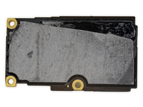
  • In addition to all these chips, we tease apart several layers of graphite thermal transfer material backing the RF board.

  • Apple says its improved thermal design gives these iPhone Pros the "best sustained performance ever in an iPhone." That's accomplished by pulling heat from the logic board straight through several layers of graphite where it dissipates into the rear case.

  • This may not seem as fancy as the liquid cooling systems we've seen in some Android phones, but it certainly must be enough to keep the super-efficient A13 cool, while not interfering with any signals traveling to or from the RF board that it clings to.

마지막으로 하지만 중요한 상단에서 다음을 발견합니다:

Toshiba TSB 4226VE9461CHNA1 1927 64GB 플래시 저장 용량

YY NEC 9M9 (아마도 가속/자이로)

이러한 모든 칩 외에도 RF 보드를 지원하는 여러 층의 graphite/그래파이트 열 전달 소재를 분리합니다.

Apple은 자사의 향상된 열 디자인으로 이 iPhone Pro들은 "iPhone 최고의 성능을 유지한다"고 말했습니다. 이는 로직 보드의 열이 여러 층의 그래파이트를 통해 후면 케이스로 분산되어 달성됩니다.

이는 일부 안드로이드 휴대폰에서 관찰된 액체 냉각 시스템만큼 멋지지 않을 수도 있지만, RF 보드를 오가는 신호를 방해하지 않으면서도 매우 효율적인 A13을 시원하게 유지하기에는 충분한 것 같습니다.

귀하의 기여는 오픈 소스 Createive Commons 라이선스 하에 허가되었습니다.