
The iPad Air 2 contains a fitting 2 GB of RAM, and has received a fitting 2 out of 10 repairability score — the same as last year’s original Air.
Yes, the Air 2’s fused glass/LCD should keep the broken glass shards more intact if the iPad takes a tumble. But it comes at a price, literally: Would-be repairers now have to replace the entire display, hiking up the cost of repair.
Aside from that, the Air 2 has a slightly smaller battery and speakers than the Air 1, and a (physically) smaller rear camera than the iPhone 6 Plus — even though it has the same megapixel count.
Teardown highlights:
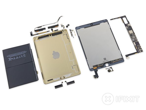
• The newly-bonded front panel is more rigid than in previous iPad models, and therefore feels a bit sturdier to pry against—however, flexing the glass still disturbs the LCD, even when you aren’t deeply inserting the pick. That being the case, the glued-down display remains the iPad’s only access point, so there’s still a risk of damaging it even when performing ordinary repairs.
- With the home button removed, we discover a single IC on the home button assembly:
• NXP Semiconductors 8416A1 Touch ID Sensor - Further inspection reveals even more ICs on the front panel assembly:
• Parade Technologies DP675 LCD Driver
• Texas Instruments TPS65143A LCD Bias Solution For LCD Panels
• When comparing the larger, bump-inducing iSight camera from the iPhone 6 Plus to the iPad’s camera, we can see they aren’t quite the same—but it’s indeed a leap in quality over the iSight camera found in the first-gen iPad Air.
• Our Wi-Fi model’s antennas now grace the top of the iPad, where previously they were ensconced along the lower edge.
• Unfortunately, the logic board is still glued in, so we call our trusty iOpener out of retirement for one more gig. Upon removal of the logic board, we are saddened to see that the Lightning connector cable remains soldered to the logic board. This makes logic board removal even more of a chore. It also means that replacing the Lightning connector basically requires replacing the entire logic board.

• The battery, once freed from the logic board’s grasp, is ready for removal. More heat and more prying free the dual-cell energy slab from the rear case. It’s not the worst battery adhesive ever seen, but it would be nice to not use plastic cards for the battery replacement, for once.
• The 27.62 Wh battery drops a bit from the previous Air’s 32.9 Wh capacity. Apple claims the same 10-hour battery life as the original Air, so more efficient power use seems to be on tap here—though early reviews seem to indicate that real-world battery life is down a bit from the previous-gen iPad.
- At last, the main course. A entire plate of chips for us! Yum.
• Apple APL1012 A8X 64-bit Processor
• Elpida/Micron Technology F8164A3MD 2 GB RAM (two 1 GB chips)
• Murata 339S02541 Wi-Fi Module
• SK Hynix H2JTDG8UD1BMR 128 Gb (16 GB) NAND Flash
• NXP 65V10 NFC Module (as found in the iPhone 6 and 6 Plus)
• Apple (Cirrus Logic) 338S1213 Audio Codec
• NXP Semiconductors LPC18B1UK (Apple M8 Motion Co-Processor)
• Maxim Integrated MAX98721BEWV Boosted Class Amplifier
• Broadcom BCM5976 Digitizer Controller
• Texas Instruments TI48WHXDP 343S0583
• Fairchild Semiconductor FDMC 6683 and FDMC 6676BZ


댓글 1개
power supply block
Anuj Kumar - 답글 공유