소개
Bigger than an iPhone 6 Plus, but smaller than an iPad Air 2. What am I? If you answered iPad Mini 3, you are correct. It's the latest iteration of Apple's miniature iPad, newly refreshed and updated—and now primed for disassembly. Join us as we tear down the iPad Mini 3.
Need more teardown talk? Follow us on Facebook, Instagram, or Twitter for the latest teardown news.
필요한 것
-
-
Pint-sized tech means pint-sized specs! Inside the iPad Mini 3, we expect to find:
-
7.9-inch (diagonal) LED-backlit Multi-Touch display with IPS technology
-
A7 chip with 64‑bit architecture + M7 motion coprocessor
-
5 MP iSight camera + 1.2 MP FaceTime HD camera
-
Wi‑Fi (802.11a/b/g/n) with dual channel (2.4GHz and 5GHz) and MIMO support + Bluetooth 4.0
-
23.8 Wh rechargeable lithium-polymer battery
-
Three-axis gyro + accelerometer + ambient light sensor
-
-
-
-
As is often the case with updates that don't really change anything, nothing has really changed yet.
-
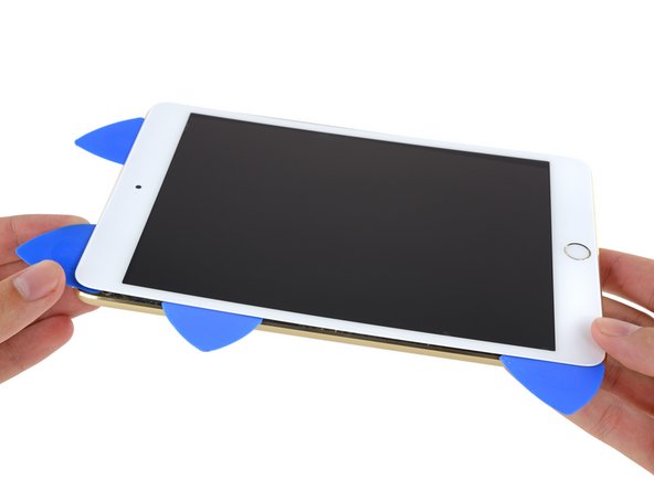
Unlike in the new iPad Air 2, the front panel glass and LCD are still separate components, individually replaceable.
-
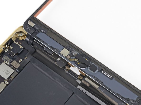
With the LCD out, we find our first and only change in construction: Some absolutely terrific home button cabling. Wow. That wasn't last-minute at all.
-
Is that hot glue?
-
-
-
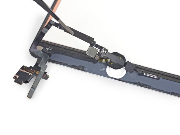
Yes—that is hot glue, holding the home button bracket to the front panel. Good luck transferring that to your replacement glass. (Which you're going to have to do, to keep the Touch ID functionality after a cracked screen repair.)
-
Looks like the cable is a bit of a nightmare all by itself.
-
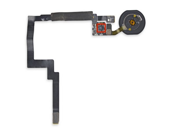
No surprises here: Touch ID in the Mini is powered by an NXP Semiconductors 8416A1 Touch ID Sensor.
-
-
-
Logic board! Let's just get to it, shall we? Anything new?
-
Apple A7 APL0698 SoC
-
Within the A7 package we find SK Hynix H9CKNNN8KTARKR 1 GB LPDDR3 DRAM
-
SK Hynix H2JTDG8UD1BMR 16 GB NAND Flash
-
Universal Scientific Industrial 339S0213 Wi-Fi Module
-
Apple 343S00004-A1
-
NXP Semiconductors 65V10 NFC Controller
-
-
-
-
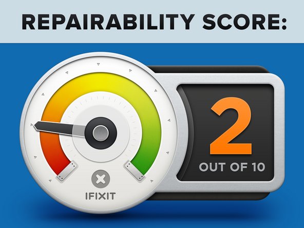
iPad Mini 3 Repairability: 2 out of 10 (10 is easiest to repair).
-
The LCD and glass are not fused together and can be replaced independently.
-
The battery is not soldered to the logic board or other components.
-
Copious amounts of adhesive hold many components in place—front glass, battery, front camera, back camera, ribbon cables—making repair extremely difficult.
-
The Lightning connector is soldered to the logic board, so don't bend its pins.
-
Removing the home button is now a much more difficult job. If you want to keep Touch ID functionality after a screen replacement, you'll have to transfer the home button to the new front panel.
-


댓글 10개
You can test the connectors are same.
I've looked better at the circuit on BRD and can tell you that iPad Mini 3 have different circuit for touch screen connector, but iPad Mini 1 and iPad Mini 2 have same circuit.
Thank god there is nothing wrong with mine,in fact it still looks brand new,but i have these guides in case something happens