소개
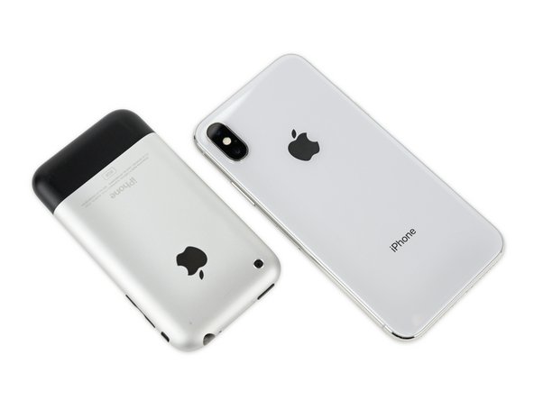
십 년 전 Apple은 최초의 iPhone을 출시했고 세상을 바꿨습니다. 오늘 우리는 Apple의 18번째 버전을 분해합니다—the iPhone X. 둥근 모서리와 edge-to-edge/전체 화면 디스플레이를 통해 우리는 Steve가 오래전에 상상했던 iPhone이라고 확신합니다—그러나 이제 그의 꿈은 실현되었는데 과연 그것이 첫 번째 iPhone만큼 영향력이 있을까요? 시간이 말해주겠지만 우리는 지금 귀하의 결정을 돕기 위해 최선을 다하겠습니다. 저희와 함께 Apple의 가장 매력적인 최신 기기를 열어서 빛나는 이유를 알아봅시다.
오스트레일리아에서 자사의 분해 작업을 호스팅 한 Circuitwise], X-ray 이미지를 제공한 Creative Electron 및 IC ID에 관한 TechInsights에 대단히 감사드립니다.
이제 오스트레일리아 상점을 개장했으며 우리가 시드니에 있다는 것은 유리합니다. 우리가 알게되는 내용은 Facebook, Instagram 및 Twitter에 게시할 것입니다. 이메일을 선호한다면 newsletter/뉴스레터도 있습니다.
필요한 것
동영상 개요
-
-
iPhone X가 나왔습니다! 다음은 이 유리 샌드위치 속을 채우는 부품들 입니다:
-
Neural Engine 및 내장 M11 Motion Coprocessor가 있는 A11 "Bionic" 칩
-
Neural Engine 및 내장 M11 Motion Coprocessor가 있는 A11 "Bionic" 칩
-
ƒ/1.8 및 ƒ/2.4 조리개 및 OIS 듀얼 12MP 카메라 (광각 및 망원)
-
ƒ/2.2 조리개, 1080p HD 비디오 녹화 및 Face ID 기능 7MP TrueDepth 카메라
-
급속-충전 및 Qi 무선 충전 지원
-
A1865 글로벌 유닛은 802.11a/b/g/n/ac Wi‑Fi w/MIMO + Bluetooth 5.0 + NFC뿐만 아니라 광범위한 셀룰러 밴드를 지원합니다.
-
-
-
iPhone은 십 년 동안 먼 길을 왔습니다—사실, 너무 멀리와서, 이 iPhone 디자인은 약간 되돌아가서 우리가 오랫동안 봐 왔던 것 보다 더 원본처럼 보입니다.
-
올해 초 iPhone 8과 마찬가지로 Apple은 iPhone X의 뒷면에서 보기 흉한 (그리고 환경적으로 책임있는) 규제 표시를 제거했습니다.
-
조니는 마침내 자신이 항상 원했던 매끈한 무기능 백플레인을 가졌습니다. 이 휴대폰이 힌트없이도 여전히 재활용 업체로 전달되어 쓰레기통에 버려지지 않기를 바랍니다.
Here in Ireland (and I guess across the EU) we have the ‘Designed by Apple in California Assembled in China’ text, the CE mark and the ‘no dumping’ bin graphic still in place.
Tom Mooney - 답글
Anyone who thinks the markings on the back of the iPhone will influence whether it is recycled (rather than the trade-in value, accessibility of recycling facility or a customer’s own environmental awareness) has probably shoved a spudger too far up their nose.
Where did you get that minty fresh first-gen iPhone? Is it part of iFixit’s collection?
I’m really glad they took out the regulatory info on the back. It simply didn’t need to be there. You know you’re not supposed to throw an electronic away.
-
-
-
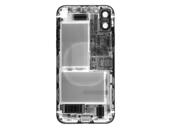
맹목적으로 뛰어들기 전에 Creative Electron 친구로부터 X-ray 정보를 받았습니다.
-
우리가 알아낸 내용은 다음과 같습니다:
-
한 개가 아닌 두 개의 배터리 셀. iPhone에서는 처음입니다!
-
최-소형 로직 보드 공간. 겹쳐진 납땜 지점을 볼때, 두 개의 층이있는 것처럼 보입니다.
-
추가 전면 센서 공간을 확보하기 위해 이어피스 스피커는 하단으로 꽤 많이 이동하였습니다.
-
Taptic Engine/탭틱 엔진과 하단 스피커 사이에는 미스터리 칩이 있습니다—하단에 어떤것이 있는지 궁금합니다!
-
-
-
이 pentalobe/펜타로브는 이상하게 완성되지 않은 것처럼 보입니다. 솔직히 하단 나사는 핀 같습니다.
-
이 나사는 나삿니 섹션을 디스플레이에서 스틸 프레임으로 이동하고 나삿니가 없는 섹션을 확장하여 엄청나게 긴 핀으로 만듭니다.
-
우리가 추측컨데 디스플레이에 약간의 유연성을 제공하는 동시에 마운팅 브래킷을 휴대폰 내부로 이동하여 강화된 Lightning 커넥터 공간을 만들었습니다.
-
다행히도 휴대폰은 크게 바뀌지 않아서 iOpener, iSclack 및 iFixit Opening Picks/여는 픽 등 전형적인 세 가지 도구를 예전처럼 사용합니다.
-
이는 여는 어려움에 큰 변화가 없음을 의미하며 우리가 알고있는 어떤 디스플레이와 달리 OLED는 프레임이 충분히 지원됩니다.
-
-
-
옆으로 열리는 iPhone은 이제 보편화가 되었습니다. Apple은 7 Plus에서 이 교묘함으로 우리를 놀라게 했지만 이제는 표준입니다.
-
이 단일 브래킷은 모든 로직 보드 커넥터를 덮습니다—이런 종류의 커넥터 밀도는 본 적이 없습니다.
-
그리고 다시 한번, 우리는 문을 지키는 pentalobe/펜타로브 나사를 지나 모든 수리에 보초를 서고있는 tri-point/3점-나사를 직면합니다.
As mentioned above.
sean -
fixed i guess
My bracket only has 4 screws - the second from top (towards the right side of the phone) is missing - I bought the phone direct from Apple on launch day. Pretty surprised! Anyone else ever had missing parts?
-
-
-
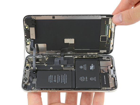
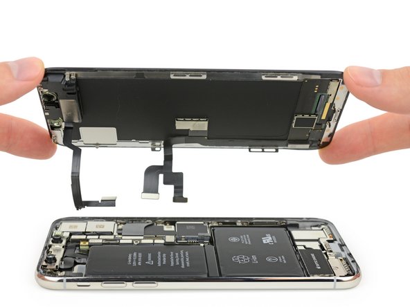
로직 보드에서 거대한 유니브래킷을 떼어낸 후, 마침내 Cupertino/쿠퍼티노의 최신 주력 제품 하드웨어를 엿볼 수 있습니다.
-
디스플레이 하드웨어는 나중에 더 살펴보겠지만, 지금은 X-레이로 만족합니다—미스터리 칩은 디스플레이에 장착되어 있습니다!
-
페이스를 바꿔 디스플레이는 들어 올려지며 전면 카메라는 남겨둡니다.
-
이 바디 샷은 X-레이로 관찰한 레이아웃을 확인합니다: 대부분의 공간은 새로운 듀얼-셀 배터리가 차지하며 로직 보드는 크게 줄었습니다.
-
-
-
이중 후면 카메라에는 연약한 부품 대한 구부러짐-방지 기능을 제공하는 것 같이 보이는 우람한 브래킷이 있습니다.
-
카메라는 후면 케이스에 추가 거품 접착제로 고정되어 흔들리지 않도록 합니다. 이 카메라는 Portrait Mode/인물 사진 모드 및 유사 기능을 최대한 사용하기 위하여 고정되야 합니다.
-
카메라 벽을 케이스에 고정하는 작은 점 용접이 카메라 하우징 커버 유리 둘레에서 보입니다.
Might that beefy bracket be made of Liquidmetal (see https://en.wikipedia.org/wiki/Liquidmeta...)? That is, is it surpisingly stiff? Apple has an exclusive license to use Liquidmetal in consumer electronics, but seems not to have used it extensively.
-
-
-
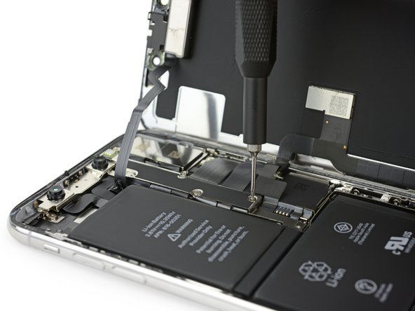
우리는 이 고-밀도 로직 보드를 마침내 분리하여 자세히 살펴봅니다.
-
소형화된 로직 보드는 매우 공간 효율적입니다. 전례가 없는 커넥터와 부품의 밀도입니다. Apple Watch에도 더 많은 bare board/빈 기판이 있습니다.
-
소형 iPhone X 보드는 더 많은 기술을 장착하며 왼편에 있는 iPhone 8 Plus 보드를 길쭉하고 널따랗게 보이게 합니다.
-
두 보드의 공간을 비교할 때 iPhone X 마더보드 크기는 iPhone 8 Plus 보드 크기의 약 70%이며—이는 훨씬 더 넓은 배터리 공간을 뜻합니다.
If that happens, how will users switch to other networks and install SIMs in their phone when they go abroad to avoid outrageous roaming charges?
-
-
-
-
Apple은 어떻게 70%의 공간에 더 많은 기술을 장착했을까요? 아, 보드를 반으로 접었군요.
-
함께 납땜되어있는 두 반쪽은 Circuitwise 호스트의 BGA hot air rework station/열풍 재작업 스테이션의 도움을 받아서 층을 분리하였습니다.
-
분리한 두 반쪽 개별 층의 전체 면적을 계산하니 iPhone 8 Plus 로직 보드 면적의 최대 135%가 늘어났습니다. 잘 했어요 Apple, 더 작은 공간에 더 큰 면적을 넣었군요.
-
iPhone X 로직 보드는 최초의 iPhone (세 번째 사진) 이후 iPhone에 장착한 첫 이-층 보드입니다.
You are missing the point. These are connecting the board physically, but there is no communication through those vias. You can see the other side of the board has all the connectors to flex. (On both boards). The third board act as a super stiffener to prevent overheating causing bending on the board. Great design!!!
Sorry Ramiro the outer row are shielding (ground) the 2rd & 3rd rows are comm lines between the boards (interposer board).
Dan -
Does the folded design take up more vertical space than the old logic board design, and if so, how did Apple account for this increased vertical space?
Was there vertical space open to begin with or does something in the design allow for more vertical space (i.e. the OLED panel is thinner)?
Thanks!
Yes, I think the OLED panel is considerably thinner. The X and 8 are pretty much the same thickness, so I think that that yes, it’s solely because of the OLED!
So Richard your assertion is that the silvered bumps all around the two boards are the vias? With a pitch of, what, 300µ?
The MacRumors article yesterday referred to an interposer between the two main boards, but I don’t see any such. Was MacRumors wrong, or am I missing something?
The outer perimeter of “silver bumps” aka solder balls is most likely all connected to ground. The rest must be signals. There is not enough cabling to support the required amount of signals between the two boards.
The interposer is still attached to the half in the top of the picture. The border of solder balls is higher than the rest of the PCB. This is required due to the night of the components on each PCB.
Truly incredible design. Passes data without cabling, affixes the two boards to each other without hardware, and creates an EMI shield without extra metal
Is that a piece of flat flex connected across two parts of the lower board? going right under the middle screw hole
It’s the ribbon from the camera’s which is poking up.
Dan -
Dan, I don't think so. Its completely sealed inside the sandwich
Thats just a kapton insulator sheet inside the sandwich. I thought you were talking about the other image.
Dan -
I believe it time to find some more of my good old LCD bonding 9703 3M anisotropic tape. That might be the ticket for servicing that motherboard. Still have some tape in stock, so my shop will service that motherboard, when parts become available.
Have a good weekend all.
Jan
How did apple manage to take out heat from their processor? I still couldn’t understand how is this working…
You are all wrong :-) look at the RF board, there isn’t a signle trace routed from the armada of solder-pads, so I’d say they’re purely mechanical & GND /tekhead
You do understand the PCB is made up of layers.
Their won’t necessary be any visible traces on the surface besides what space is there! It’s so packed the lines would need to be buried inside the layers. One of the functions of via’s is to bring signals up and down the layers, clearly Apple is leveraging this here through the interposer board.
Dan -
@kyle - Found a good image set from Tech Insights! Here’s the side views http://www.techinsights.com/uploadedImag... and http://www.techinsights.com/uploadedImag...
There’s a lot of need for intercommunication between the RF and the main CPU. There’s no other interconnect between the two boards. The perimeter vias have to be a communication bus.
Kyle Wiens - 답글
-
-
-
첫 번째 반쪽:
-
SK Hynix H9HKNNNDBMAUUR 3GB LPDDR4x RAM에 계층화된 Apple APL1W72 A11 Bionic SoC.
-
Apple 338S00341-B1 전원 관리 IC
-
TI 78AVZ81 배터리 충전기
-
NXP 1612A1—1610 tristar IC의 신형으로 보임
-
Apple 338S00248 오디오 코덱
-
STB600B0
-
Apple 338S00306 전원 관리 IC
What are those “white stickers” in different shapes on the board? Are they the typical for checking water damage? Are the same shapes stickers related to each other in any way? Function?
Some of these components have a polarity. The white or black dot or a triangle denotes positive or anode end of the cap or diode.
Dan -
I think those are inductors, and the white spot indicates the right direction for them to go on the board.
Which is A11 Apple processor module part number, on same package row as SoC die designation APL1W72? The A11 Apple processor module part number has a format 339S004xx. The A11 photos are without sufficient contrast and difficult to read.
No help on A11 Apple processor module part number in this analysed iPhone?
Dimitar -
Is it me or are all the surface mount capacitors misaligned on the far right end? One is barely making contact with the pad. It’s like someone fudged it with their thumb picking it up.
Ian Melzer - 답글
I think that happens when you desolder it with hot air. It heats up the whole board.
which one of these chips are the thermal monitor? I have a damaged IPhone X that says the thermal monitor is dead.
I would be surprised if there is a separate chip for thermal monitoring. It’s more likely a function buried in one of the other ICs, probably one of the power management devices.
-
-
-
Apple / Murata USI 170821 339S00397 WiFi / 블루투스 모듈
-
Qualcomm WTR5975 기가비트 LTE 송수신기.
-
Qualcomm MDM9655 Snapdragon X16 LTE 모뎀 및 PMD9655 PMIC. 그러나 Apple은 모뎀을 이중-공급하고 있으며 TechInsights는 A1901 모델에서 Intel XMM7480 (PMB9948)을 발견했습니다. 모뎀이 기가비트 속도 지원 가능하더라도 Apple은 Qualcomm 부품에 지원하지 않습니다.
-
Skyworks 78140-22 전력 증폭기, SKY77366-17 전력 증폭기, S770 6662, 3760 5418 1736
-
Broadcom BCM59355 무선 충전 컨트롤러
-
NXP 80V18 PN80V NFC 컨트롤러 모듈
-
Broadcom AFEM-8072, MMMB 전력 증폭기 모듈
Vic Lau, Qualcomm makes good chips at good prices, so there isn’t any reason Apple shouldn’t use them.
Yes, there is. They're suing each other.
If apple moves away from Qualcomm we can definitely expect a higher price tag on the next iteration of the iPhone
DAXimus -
The suing didn’t stop Qualcomm to get enough order apparently.
On the contrary,a higher price for customers to purchase iPhoneX seems to be the only result.
Theres more to it than the chips, It appears there are some licensing payments owed. Here’s a bit more Apple may completely drop Qualcomm as a modem supplier on future iPhone models
Dan -
Both those chips are present in Iphone 8 plus as well. They are just in different locations. Check step 10 in Iphone 8 plus tear-down.
Actually both the chips are required. MDM9655 is a baseband modem, and WTR5975 is a RF transceiver.
my Logic board has some damages to the circuit. I was thinking about buying another logic board (say iCloud locked) and transfer all if these chips. Will it work? Has anyone done it?
bijaya.pun - 답글
-
-
-
그리고 로직 보드 샌드위치 바깥쪽에:
-
Toshiba TSB3234X68354TWNA1 64GB 플래시 메모리
-
Apple/Cirrus Logic 338S00296 오디오 증폭기
Kapton tape on the underside for insulation, yeah
looks like the backside of the reader
anyone can tell that the storage its a TLC or MLC?
leartzajmi - 답글
And what to say about those two capacitors a bit off their solder points, almost touching the capacitor next to it ? Should’ve been failed in quality control, or visual inspection at least, no ?
Or …. Could it be the heat from you guys separating the boards, that made the components wiggle a bit and shift from their correct placement ?
The second one. ;) We’re doing this for the first time, often under less than ideal conditions, in a pretty big hurry. People who are more skilled and patient than I am can separate the boards and solder them back together flawlessly.
-
-
-
그래요, Apple이 PCB 샌드위치를 만들었는데 이는 어떻게 작동합니까?
-
여기 A11 SoC는 메인 보드 중앙에 자리 잡고 있습니다. X-레이 사진에서 보드의 3D 구조를 파악할 수 있습니다. 가장자리 주위의 실린더들은 두 보드를 연결하는 땜납으로 채워진 구멍들입니다.
Dan, most through-hole vias are hollow.
-> iFixit,
look again, there are no traces routed from those, so I don’t think any data is travelling through those. It’s just ground.
any relevant high-speed bus wouldn’t work well routed in that manner.
main board is the “computer“ where all the flexes come in to connect to screen & peripherals.
the rf-board is purely networking so very few wires has to connect between the main ARM and that board.
Albert, Review the comments in Step9 there is no other means for the two half to communicate with each other other than the vias and yes some are shielding (ground)
Dan -
Lel. Yeah. Those are just via stiching for shielding.
Maybe vias are security related. PCI homologation request for tamper-proof protection against encryption keys reading strait from RAM.
I think you are right! but I’m not sure that which chip to process security function.
-
-
-
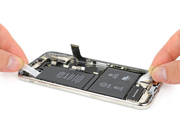
새로운 듀얼-셀 배터리에는 8 시리즈의 짧은 당기는-탭과 비슷한, 완전히 새로운 방향의, 당기는-탭 네 개가 있습니다.
-
이 휴대폰은 10.35Wh (3.81V 2716mAh) 배터리를 장착하고 있으며 10.28Wh 8 Plus 배터리를 능가합니다—하지만 여전히 Galaxy Note8의 거대한 12.71Wh를 쫓아가는 중 입니다.
-
듀얼-셀 디자인은 용량-개선보다는 공간-활용 개선에 가깝습니다. 셀 두 개는 로직 보드를 축소하여 남은 공간을 최대한 활용하여 보다 창의적인 모양과 배치가 가능합니다.
It might be my age showing but what type of Li-Ion supports charging up to 4.35 ? (I mean .. there’s the type that goes up in flames but .. ?)
It is just a more stable battery that can handle higher voltage without damage. Even my Cubot Note S has 4,35V max voltage battery (4.150 mAh).
Okay so I use this phone for all the photos of appliances that we take at Jackson Appliance Repair Company. The question I have is— is the battery itself waterproof? Or is the phone waterproof (protecting components inside) when it’s fully assembled?
The device is waterproof. Batteries really can’t be made waterproof as they have exposed contacts which when shorted would be dangerous depending on how conductive the liquid was (i.e. salt water).
Dan -
-
-
-
Face ID 기능을 기억하나요? 이례적으로, 우리는 휴대폰을 분해하기 전에 실제로 테스트를 했습니다. 자사의 IR-지원 비디오 카메라가 도트 패턴을 잡기에 충분히 빠르지 않지만 조명은 괜찮게 잡았습니다.
-
역사 시간: 옛날에, Microsoft는 Kinect라는 멋진 공간 센서를 만들었습니다. 이에 동력을 제공하는 적외선 도트 매트릭스 기술은 이스라엘 기술 회사 PrimeSense가 개발했습니다.
-
Apple은 2013년에 PrimeSense를 3억 6천만 달러에 인수했으며 그 이후로 수 억 달러를 더 투자했습니다.
-
한편, 휘청거리던 Microsoft는 허둥지둥 Kinect 2의 새로운 센싱 시스템을 개발합니다. 이제 iPhone에는 깊이 센서가 장착되어서 아마 사람들은 드론에 부착하려고 할 것입니다.
@kyle tell your design team to add a play button over the image, people can easily miss that it’s a video. I thought it was just an image, but saw the comment about he enjoyed watching the video - so i hovered my mouse and then that’s I figured it’s really a video. :)
It’s IR. Human eyes can’t see it, so unlocking with Face ID is essentially just staring at it, and from the user’s perspective, it magically unlocks. No visible flashing here!
Jody, the flashes are invisible to the human eye. In the video you can hear the guy with the phone asking if the cameraman can see the flashes, because you need a special camera to view them. It’d be like staring into the end of a TV remote control and pushing buttons.
Not for me. I can see infrared easily.
Esa luz que nosotros no vemos, sera dañina de tanto uso ?. Porque desbloqueamos el telefono muchisimas veces al dia.
That light that we do not see, will be harmful of so much use? Because we unlock the phone many times a day.
Here’s a good vid on the FaceID projector lighting up someones face: https://youtu.be/OvVKnC6gGtg Jump to 5:50 to see it.
so why MS did not buy ++PrimeSense?++
Having designed a lens system for Occipital’s Structure sensor (which is also a Prime Sense derivative). The structured light emitter, which is actually a laser; vibrates to create the pattern that bathes your face. I am pretty sure the structure light source does not have the power to do anything besides scan your face, but also the infrared camera is lens system is probably tuned for 300 mm-500 mm unlike the Kinect(1), ASUS XTION or PrimeSense’s own early versions, which have a much longer range. If anyone is interested in doing more than just face scanning, check out Occipital’s website.: https://structure.io/ .
i wonder who makes the sensor subassembly - that must be a very intricate design; tying the processing and interface to the VCSELs that generate the light powering the activity
-
-
-
우리는 최상의 휴대폰에서 매우 기대되는 TrueDepth 카메라 시스템으로 관심을 돌립니다! 이 시스템은 센서 팀을 모아 X에 안면 인식을 제공합니다.
-
1단계: 디스플레이에 내장된 플러드 일루미네이터가 적외선 (IR) 빛으로 얼굴을 비춥니 다.
-
다음, 빨간색으로 표시된 전면 카메라는 얼굴의 존재를 확인합니다.
-
그 다음, 가장 오른편에있는 IR 도트 프로젝터가 얼굴 위로 점 격자를 투영하여 3-차원 지도를 만듭니다.
-
마지막으로, 왼편의 IR 카메라가 이 지도를 읽고 데이터를 휴대폰으로 보냅니다.
-
X는 후드 아래에서 매우 빠르게 소프트웨어 마술을 사용하여 이 모든 정보를 모아서 귀하인지 또는 귀하의 악한 쌍둥이인지 알아냅니다.
Surely the ir camera senses the ir flood projector, not the standard camera…
There are three IR light sources used: The small pencil beam to see if the phone is face down or next to ones face (proximity) which uses the camera as the sensor (located just to the left of the speaker slot from the front). Then there is the flood illuminator which lets the camera ‘see’ if you are there (to discriminate there is a face present) just to the right of the camera. The third is the dot projector (on the right side of the speaker slot) to ID you. The same camera is used for all three functions no special IR camera here.
Can I buy that TrueDepth system?
JJ Delisle - 답글
Has anybody figured out, if this part is replaceable? I hope this isn’t handled like the TouchID which is locked to the logic board?
-
-
-
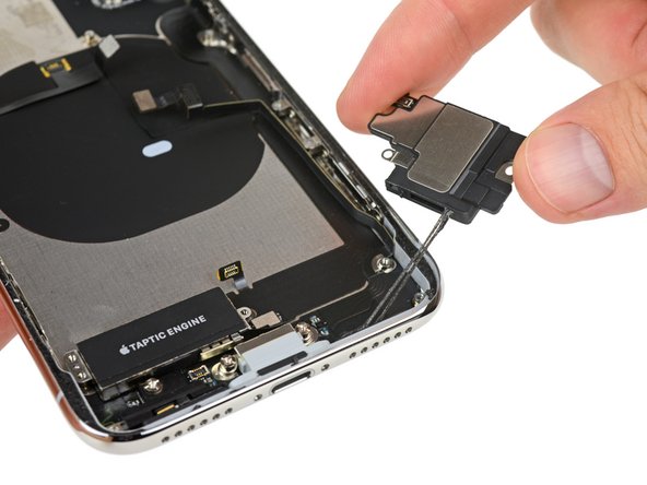
저기 끝이 보입니다, 우리는 후면 케이스의 나머지 부품을 통해 전원을 공급합니다.
-
이 첫 번째 작은 브래킷은 스프링 커넥터 및 EMI 접지 핑거로 덮여 있으며 뒷면에 리본 케이블이 붙어 있습니다.
-
다음으로 분리하는 것은 포트 주위의 끈적거리는 방수 접착제로 가득찬 하단 스피커 인클로저입니다.
-
마지막으로 Taptic Engine/탭틱 엔진과 유명한 기압 벤트가 해제됩니다. Apple의 Taptic Engine/탭틱 엔진은 여전히 선형 오실레이터 진동 모터입니다.
Are there two speakers at the bottom?
Nope just the one lower speaker. The second speaker is mounted to the upper portion of the display assembly.
How is vibration motor installe, it is glued or screwed?
A: Screwed. ;)
Do you sell replacements of the little bracket that is covered in spring connectors and EMI grounding fingers, and has a ribbon cable stuck to the back? As I was removing my screen to prepare for a replacement I saw that it had some damage. I don’t want to purchase a replace screen and find that it won’t work because of the damage to this part.
Caleb for some strange reason iFixit do not sell the EMI Grounding Finger plate nor do they sell the wifi flex cable that is attached to the underside of that plate. I had to go to Amazon to source a replacement for both. I think they should also stress how delicate those grounding fingers are, they are like tissue paper and can be damaged very easily if touched so take extreme caution when removing and reinstalling the plate and the attached flex cable.
Do you have links?? I can not find it.
There are two screws immediately below the taptic engine. Neither the PH000 or PH00 screwdriver works. Anyone know what screwdriver it is?
Nice and informative post very helpful thanks for it, MS OFFICE 2019 MAC with lifetime license 70% Off.
Does anyone know the purpose of this bracket "covered in spring connectors and EMI grounding fingers"? What would be the possible side effects if it was damaged?
-
-
-
언제나 컨디션이 좋은 우리 분해도 엔지니어는 Lightning 커넥터를 분리하는 이중 핀셋 기술을 보여줍니다.
-
충전 케이블 흔들 블루스를 겪는 사용자에게 희소식: Lightning 커넥터는 프레임 측벽에 나사로 고정하는 더 넓은 브래킷으로 더욱 강화되어 보입니다.
-
또한 앞서 본 것처럼 외부 pentalobe/펜타로브 나사가 디스플레이를 지나 끼워지는 through holes/스루홀/관통 구멍이 있습니다.
I don’t think it really matters. Apple’s Lightning Connector is double sided, so EVEN IF they DO have contact points on both sides, they probably would have wired them together anyway.
The Lightning connector IS double sided, however the pins are NOT NECESSARILY physically tied together in the connector; ergo it actually supports 16-pins, not 8. So it DOES matter. A double-sided port could hypothetically support Thunderbolt, or 2 USB3 channels. And we have seen, inexplicably, a double-sided port from Apple before in the iPad Pro. A fully 2-sided Lightning connector/port could be functionally as capable as USB Type-C, minus the legacy USB 2.0 lanes. (The Type-C connector ALWAYS maintains a legacy USB 2.0 pair; Apple would have no need for that legacy combination if Thunderbolt was their forward-looking target.)
Scott,
Apple has already defined the connector https://en.wikipedia.org/wiki/Lightning_... I doubt they are going to mess it up making it polarized directionally at this point.
Dan -
There are 2 separate parts here. One is the Lightning connector and the flex cable under it is the loud speaker flex cable.
-
-
-
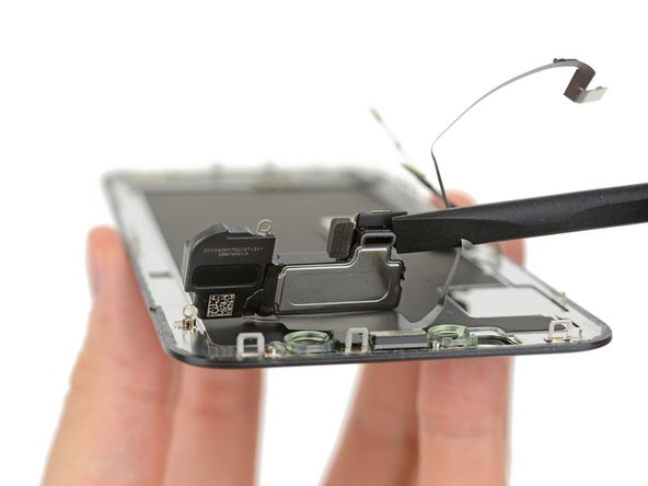
주 어셈블리를 조각조각 분리한 후 우리의 관심은 디스플레이로 돌아갑니다. 가장 먼저 눈에 띄는 것은 디스플레이에서 사운드를 전달하기 위한 멋진 덕트로 새롭게 디자인된 이어피스 스피커입니다.
-
상단 디스플레이 부품을 조심히 추출하면 지금까지 보지 못한 가장 복잡한 상단 디스플레이 부품 조합이 나타납니다. 라우드스피커, 마이크, 주변 광 센서, 플러드 일루미네이터 및 근접 센서가 모여 있습니다.
-
모든 모듈식 조각을 분리하고 나면 덩그러니 디스플레이만 남습니다.
So what was that mystery chip first shown in the x-ray pictures?
Where can I find a replacement upper display? Accidentally tore my wire ribbon slightly…
-
-
-
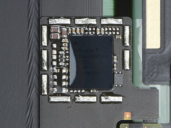
그 미스터리 칩을 볼 시간입니다! TechInsights 친구들로 부터 약간의 도움을 받아 디스플레이 뒷면의 보호막 아래를 살펴보고 다음을 발견하였습니다:
-
BCM15951B0KUB2G 라벨 Broadcom 터치 스크린 컨트롤러.
-
또한 함께 따라온: 우리가 전에 보지 못했던 새로운 STMicro 기기 10 THADT733 X-139U 라벨 OLED PMIC.
The ST is more likely a boost converter, look at the inductors around it.
Too few pins to be a oled display-driver
-
-
-
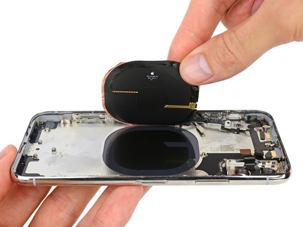
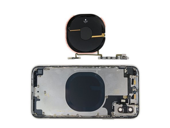
X의 금속 뼈대에 도달하는 중 우리는 이 밀도 높은 퍼즐의 또 다른 친숙한 부품을 발견했습니다: 무선 충전 코일.
-
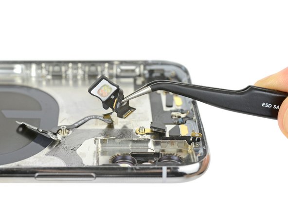
그리고, 볼륨 버튼, 링/사일런트 스위치 및 미확인 센서 브래킷을 포함, 연결된 모든 것.
-
또한 전화 상단의 다른 다-기능 케이블을 벗겨냅니다. 이 어셈블리는 옛날 iPhone 처럼 quad-LED True Tone 플래시 및 전원 버튼의 본거지 입니다.
Is the Qi coil that needs to be unobstructed for wireless charging just the center circle the ribbons are attached to or is it the whole unit?
You can see the coil in step 3 x-ray images.
Just the big black coil.
Is there anything special with the charging coil? Do you think they are being modest and when airpower comes out it will blow away qi coils?
-
-
-
보너스 라운드: 새 iPhone X의 후면 유리가 깨지면 어떻게 됩니까?
-
열이 많이 많이 난 후, spudger/스퍼저는 집어 넣어 치우고 Jimmy/지미를 뽑아들었습니다. iPhone 8 및 8 Plus와 마찬가지로 X는 심하게 접착된 후면 패널을 가지고 있습니다.
-
조심히 Jimmy/지미를 사용한 후에도 해결이 안됨: iPhone 8의 일체형 후면 패널과 달리 카메라 범프는 후면 유리와 겹치며 아래의 금속 프레임에 꼼꼼하게 용접되어 있습니다.
-
이 클래식 hand-stuck-in-cookie-jar/과자-통에-끼인-손 상황에서는 손을 (카메라 범프) 잘라내거나 과자 통을 (후면 유리) 부숴야 합니다. 이런.
Could you show the other side of the stainless shell? Is the glass apple logo and lettering at the bottom printed on the backside and glass layer over top?
Yup, same as the 8, you can see the bare inside of the glass here.
looking for this solution
How was the camera bump removed?
Ivan Beatz - 답글
Destructively. It’s welded into place from the inside.
I find using a small flat head at each one of the weld points and rocking it left and right with a little force helps break the weld with less trouble than trying something large like a jimmy tool.
I opened the phone, removed the rear cameras, flash, logic board and battery, then wedged something underneath the rear camera bracket (which is spot welded to the camera bump) to break the spot welds to the camera bump. You’ll end up destroying the bracket (my replacement glass came with a new bracket and camera bump/lens) the bump will literally fall out once done. The rear glass can then be removed and replaced, then fit new camera bracket (and camera bump if damaged when removed).
Feel like doing a walk-through on this with photos for those less-inclined to break their new iPhone just because of a smashed back panel? :D
Absolute joke. After having spent all day painstakingly removing every single glass shard from the rear I find out that the bloody rear replacement glass doesn’t fit over the camera bump anyway…
Is there not a version that just fits over the bump even if it leaves a tiny gap ??? There is no way people will want their cameras/mics butchered. Failing that, it seems a bit excessive to strip down the entire phone just to remove a welded bracket. Frankly it is RIDICULOUS and I have been doing smartphone/tablet repairs from day 1.
It’s my own fault for not researching the subject. I wrongly assumed it was like previous models where it’s just held in place with adhesive tape.
This same kind of thing happened to me when the iPad airs came out and I thought it was still possible to do ‘glass only’. I think the only way I will learn is from not doing Apple repairs anymore!
Anyway well done Apple for catching me out yet again…..
Further update… Managed to find a seller on eBay who sells the rear glass covers with a slightly larger camera hole so it fits straight over the bump/lens. While this isn’t a perfect solution as there will be a bit of a gap it does makes it a million times easier and actually becomes feasible to do this repair (if you don’t mind hacking away at glass all day!).
My initial outburst was mainly because I was doing this job as a gesture of good will for someone and just assumed it to be straight forward. If it was my own phone or that of a close family/friend I would have just stripped it all down and done a proper job.
Hope this helps someone!
I use glass from aliexpress with normal hole with separate camera holder. If you put big hole glass you have the water resist problem.
Zeljko -
-
-
-
우리는 귀하께서 22-코스 분해 식사를 맛있게 드셨기를 바랍니다. 매우 영양가가 있는 분해도 입니다.
-
iPhone 8 또는 iPhone 8 Plus 분해를 놓쳤다면 살펴보고 비교할 수 있습니다. 또한 스마트폰 수리용이성 목록에서 이전 기기 점수를 살펴보세요.
-
유용한 도우미 Circuitwise, Creative Electron 및 TechInsights에 다시 한 번 감사드립니다!
-
- 디스플레이 및 배터리 수리는 여전히 설계의 우선 순위입니다.
- 깨진 디스플레이는 생체인식 Face ID 하드웨어를 분리하지 않고 교체할 수 있습니다.
- 접착제보다 나사 사용을 선호하지만—표준 Phillips/필립스 외에 Apple-전용 드라이버 (Pentalobe/펜타로브 및 tri-point/트라이-포인트)를 준비해야 합니다.
- 방수 조치는 일부 수리를 복잡하게 하지만 물에 의한 피해 수리 가능성은 낮습니다.
- 까다로운 케이블은 관련없는 부품을 복잡한 어셈블리로 묶어—많은 비용이 들고 교체가 까다롭습니다.
- 전면과 후면 유리는 깨질 가능성을 두 배로 높이며—후면 유리가 깨지면 모든 부품을 분리하고 섀시 전체를 교체해야 합니다.


최종 결론
수리 용이성 점수


(10은 가장 쉬운 수리를 뜻합니다)
다음 번역가들에게 특별히 감사 드립니다:
85%


이 번역자 분들은 저희가 세상을 수리하는데 동참해 주시는 분입니다! 기여하시겠습니까?
번역 시작하기 ›
댓글 146개
Incredible and dense tech inside this iPhone - thanks ifixit!
Wow! So exciting!
Hello,
Could you give us more info about NFC antenna localization? I suppose it’s on top of the back panel (to avoid conflict with Qi )
Thanks
It’s the top bezel itself, as always.
Tom Chai -
From Iphone 6 to XS Max, its always been on top?
Exactly! Given the amount of effort they put into shrinking (or folding) certain parts, it’s great to see they’ve put in the same effort to not make it harder to repair. That any modern smartphone will never receive a 10/10 score due to the design choices is acceptable, so I’m happy to see there’s still a reasonable way in. Not like some tablet/laptop hybrids that are horrendous to even open up; yes I’m looking at you Microsoft!
is the face id hardware programmed to the phone like the touch ID was? that would make replacing it impossible by 3rd parties.
i know its not connected to the screen, but still it may be a common repair like it is now.
There isn’t really a reason why replacing the True Depth sensors should be a “common replacement” like the home button was. The home button had to be replaced because it was a physical piece of hardware that was pressed millions of times before failing. The True Depth sensor should fail rarely since it is protected under glass and won’t be hammered on constantly.
Very good! Finally different in the interior, the previous models were all the same!
Question which iPhone X version is this? with 2 Qualcom chips it looks like it is the Model A1865
We analyzed the A1865. TechInsights opened up an A1901.
Apple claims that in order to make the screen curve with the edges, they had to fold part of the OLED screen over to hide the display driver right under the screen. Would you be able to verify that?
yes, there was an animation in the promo video. Looked weird. I’d like to know how they get the cutout in there.
And how do the cutout pixels account to the display resolution?
Andi -
Yes I saw this too, can you investigate more into the OLED display? In the video at 0:30, Jony Ive says “the custom OLED panel was engineered to fold and seamlessly combine with the external surfaces.” Their computer rendering really makes it appear there are hundreds of hidden pixels being illuminated. https://youtu.be/K4wEI5zhHB0?t=30s
Sweet! I’m actually impressed by the efficiency of this.
The picture of the sandwich board is tilted and out of focus. Please retake from directly above
Hey Mitch! We have top down photos of the logic board in steps 9, 10, 11, and 12! Check them out! The photo in step 13 is meant to describe depth, so the angle the focus on the chips inside is intentional!
Please post XRay Wallpaper of the iPhone X! You guys are the only ones that do it right!
Just snag the xray ‘wallpaper’ off the enlarged picture above… o.O
From a boardlevel repair perspective I sense this is mostly game over.
Separation of the two layers requires an amount of heat applied to the whole structure pretty much all soldering folks would consider unsafe including myself.
Lets all hope very strong that this design improves mechanical stability to a point where we wont have breaking solder joints any more and improved circuitry preventing most common damages. The level and style of catch up game with the repair industry apple plays here is disconcerting.
After settling with recent macs not to be considered buyable because of &&^&^$^ all components being soldered in and tethered added to ridiculous toylike features driving stupid prices now the iPhone is also beyond what I am willing to accept for such money.
Its depressing to see how fast apple from year to year is becoming more about profit and money and less about tech and users.
I wonder how long I have to wait until some other player comes up with a real alternative in terms of user experience.
Yes i agree, what they did will make repairs harder you can see in this pictures some components moved from their place after separation which is a bad outcome.
Have you considered the Essential Phone? It seems like they may have something special over there…
Gino J -
I have to agree. I started out in 1980 with my bsee degree repairing Apple 1’s 2’s and 3’s with an oscilloscope, soldering iron and the latest copy of the ic circuit handbook. I have not been thrilled about Apples progression from everyman’s or women’s mac to unserviceable sometimes throw away stuff that needs cottage industries to support what they can, when before it was mainstream repair with dig this, a service door!.
@Ross Elkins: The Apple 1, ][ and /// were designs based on 7400-series TTL logic. Do you have any idea how big, power-hungry (and expensive!) devices like the iPhone would be, if they were designed with 7400 chips? If it would even be possible (which I seriously doubt), the PCBs stuffed-full of TTL logic would easily cover a football field, would require a 1000A power supply, and would cost $100,000 (or more)!!!
For you to even mention the repairability of stone knives and bearskins designs (no offense meant to Mssrs. Wozniak and company) like the first few Apple computers in the same breath as state of the art, massively-integrated product designs like the iPhone X strongly suggests that you wasted your money on that EE degree; because you certainly haven’t been keeping up with technology, even at a lay,an’s level.
Yes, serviceability has definitely lost ground to compact design over the years. There are trade offs everywhere and either we carry around a brick with a removable back panel for component repair/replacement access, or have the smartphone design we do today where it's practically an extension of our body. I'm for the latter.
I do love iFixit teardowns though, daring to go where no one is intended to.
I salute you, iFixit!
gamma
@atomicsymphonic Umm… you have to FREEZE it to get it open! Essential Phone Teardown It got a repairability score of 1.
Does the bottom left of the phone still just have a dummy panel covering the speaker grill?
If you’re thinking of the barometric vent, then yes! You can see it in the third image on step 17.
It looks like the mysterious chip was attached to the lower speaker…any idea what it is used for?
It is still mysterious!
Does the mystery chip possibly contain the data for the user’s facial recognition? Apple said that data would be stored on the phone only - and nowhere else - out of privacy concerns.
HL Dash -
Were you able to verify that face recognition still worked once the phone was re-assembled?
Cindy Leek - 답글
Facial Recognition works. But proximity sensor has to be swapped over to maintain Face ID after a screen swap.
iv tried today to swap screens on two iPhone X without swapping over any parts, just the screens and Face ID stopped working on both. ill try later to swap the proximity sensor to see if that fixes the Face ID.
roy -
I swapped two screens from one to the other on the iPhone X and Face ID stopped working on both. ill try later to see if swapping the proximity sensor fixes the Face ID not working.
roy -
Should be much easier to repair without the virtual touch id button.
John Knirr - 답글
this looks like a science fiction movie, very big WOW
Be nice if the person breaking down the phone, or at least the one who writes up the Teardown, had some engineering training, some of the text above was completely unintelligible, unscientific and used wrong terminology in descriptions. Apart from that, though, great! LOL
And you’re perfect in everything that you do right? If you’re so smart you should have filtered through all type O’s and kept your rude post to yourself, JACKASS!!
Stay tuned ;)
The next thing to go is the nano sim tray for sure it's so large compared to the logic board.
Apple’s almost definitely going to replace it with an eSIM in the next model. I sure hope so. https://www.blog.google/products/project...
What about the screen essentially folding backwards on top of itself? I was wondering about that in a tear down like this. Here’s what I’m referring to: https://boygeniusreport.files.wordpress....
We picked up an A1865 in Australia!
Maybe I missed it, but did we find out what the chip next to the speaker is? It was called out with a green box on the X-Ray in the 3rd step. I don’t think i saw the explanation.
gregkramer - 답글
I believe you’re talking about the chip in Step 20!
Just a guess, but the “Unidentified sensor bracket” in Step 21 could be related to Apple’s new leather folio case which wakes the phone upon opening and sleeps upon closing.
I’m sure the IR proximity is what does that
Dan -
It’s unlikely to be the proximity sensor doing this, as then it would work with third party cases as well, not just Apple’s and would do something similar when just covering or uncovering the screen.
In the iPhone X promo video from Apple, we can see the OLED screen is curved under itself, which I’ve read is to ensure a consistent light all the way to the edges of the phone.
_
I’ve looked above a few times at the various steps but don’t seem to find any reference to details on the OLED screen, which you’d imagine is a very important part of any smartphone.
_
iFixit, can you please add a 24th step that goes into detail on this? I can see from a couple of comments above that I’m not the only person wanting to know.
_
Thank you for your incredible work!
_
Regards
_
Alex
Any idea who they are using for the Qi charging IC?
Apple made there own coil. It has the apple insignia on it
zachary -
Are you able to put the phone back together and have it still be functional, or does this tear-down destroy the phone?
The degree of consolidation for functionality in the circuitry is unprecedented! State of the art.
Very nice, good explain
Very informative! I love your site!
Ram wasn’t mentioned this year? What is it? How much ram?
3 GB of RAM in the A11 chip
Dan -
Face id only works if the phone is vertical.
John Knirr - 답글
Any commentary on the antenna design and how it compares to 8/7 (plus/nonplus)?
iPhone X is the same wireless charging hardware design like iPhone 8 ? any difference?
Excellent site do you only describe etc phones?
IFIXIT covers many different products review the other tear downs here: https://www.ifixit.com/Teardown
Dan -
I just hope no costumer comes in with a broken rear…
thanks lot for all ifixit team
So amazing PCBs layout!
Would appreciate your comments about the Snapdragon X16 Modem. Have the aireals been disabled by Apple in a smilar fashion to the way they were disabled on the Iphone 8 and 8Plus model 1865? This seems to be an important issue? Jack
This is too cool ! Do you have data on which parts are best in class the industry offers ?
lol Apple REVEALED! KUDOS IFIXIT
Hi, I know that the iPhone X supports the auto sleep/wake function, as on iPads, using wallet covers like the original Apple Folio one, so I think there should be magnets inside the phone, is that true? If yes where they are? I saw tons of wallet covers on eBay that are sold as "magnetic" but they don't say if they support the auto sleep/wake function, anybody has tried one of these? Thanks
Fantastic teardown guys!! I am curious about the stainless steel ring around the frame. It does appear that it’s composed of 4 distinct pieces due to the seams between.
Can you guys comment on how they’re connected to each other as well as the backplane?
It does make me wonder on the Space Grey version - are the 4 pieces PVD coated before they’re joined or after?
I work for a phone company and we are getting these phones returned by same group of people, they take the phone out then 24 hours they return it, the boxes are open but the phones are still in the plastic seals, it there anything that can be done to these phones they look as good as new but my gut is saying something has been done with the phones.
Hello, please, iPhone X has two or only one bottom microphone? On picture is only one, and iPhone 6S, 7 have two.
How the on screen finger print works? what kind of part’s it need to execute?
There is no in screen touch ID. Just Face ID, and there’s no fingerprint reader anywhere on the phone.
Hi, please, where is fourth microphone at bottom of the phone? Integrated in speaker assembly? All phones since iPhone 7 has 4 microphones, and i counted there only 3.
Where can I get an iPhone X chassis to fix my phone
Hello were can i buy chassis for iphone X thanks
unidentifed censer? They are spying on us lol
Wheres the antenna located? Top Bezel?
What’s the size of the back camera sensors? I want to compare it to my older dusty point and shoots.
Hi ifixit team,
bluetooth and wifi module can be replaceble?
What do you do with the phones from your teardowns?
Liam Judge - 답글
@ltjjudge Lots of things—after the teardown we go to work writing repair guides, so teardown phones and components get used for guide photos, parts compatibility testing, etc.
can anyone please tell me is there a slight flex or compression in iPhone X screen when pressed a little hard in the centre of the display. Also please tell me if u hear a hollow tap in the middle region of display compared to corners when u tap it with moderate force?
My iPhone X sim port was open and it fell inside the water and turn blank on the screen what can I do to solve this problem
Hi iFixit team,
At step 21 , there’s a rubber / silicone casing around the camera flash , which (I suppose) helps with water / dust isolation. I’m missing mine (repair shop probably “forgot” to put it back in). Any idea where I could get one?
Thanks a lot!
Marek
Could anyone unfold the logic board or is it really complex?
Getting it apart is very straightforward if you have a good hot air station. (There are numerous how-to videos on YouTube at this point.) Putting it back together in good working order is significantly tougher, but do-able.
Si cambio la placa del iphone x el face id deja de funcionar?
Can u tell me where is the gps chip in iphone x
aman verma - 답글
Yeah, like as my new iPhone adapter
Grazie, precisi e meticolosi.
Face ID no set up
Merci pour cette vue d’ensemble et merci pour la traduction
Ich habe diese Höllentour durch - ohne Teardown und Anleitung. Display und Rückseite waren gebrochen und mussten neu. 6 Stunden fummeln und fluchen später war das Ding fertig. Besonders unlustig: Mehrfach überlappende Kabel und Bleche, dazu zig verschieden große und lange Schrauben. Das bekommt Apple auch NIE in den Griff sich auf 2 Schraubengrößen zu einigen. PS: Rückseite geht bei über 180 Grad ab wie Butter. Vorher aber das gesamte Gerät bis zum letzten Teil entkernen.
Someone help me with this, i try to replaced my battery on my iPhone, everything is perfect except my phone can’t catch the wifi well. Someone help me please
Where are the cellular antennas?
All, do you know where is the GPS located?
Which iPhone X model number are you investigating?
Dimitar - 답글
I think we can safely assume it’s the global A1901 model. Both other models are country specific according to EveryMac.com: A1865 for China and A1902 for Japan.
addvariety - 답글
A1865 is for US Verizon and Sprint too
Sam Sun -
On-cell display or in-cell display?
Albee Einstein - 답글
1901 is not global. It’s the GSM only version with the inferior Intel chips. The Qualcomm 1865 is the global/unlocked version.
Xiao - 답글
Where can I find a X with out LCD, Digitizer, screen?
Grant Nord - 답글